Metallographic preparation of microelectronics

Due to their size and complexity, preparing microelectronic components for metallographic analysis can be challenging. This guide outlines the special techniques and equipment required to ensure effective and accurate controlled material removal in microelectronic samples, with reproducible results.
The main characteristics of microelectronics
Over the past 25 years, the development and production of electronic equipment has advanced rapidly. Previously, electronic equipment was large and bulky, with most electronic components individually wired on large printed circuit boards (PCBs).
The development of integrated circuits (IC) has made the miniaturization of microelectronic components possible. ICs are smaller, more reliable, cheaper to make, and better performing than the wired versions. ICs combine active components (such as transistors and diodes) with passive components (such as resistors and capacitors) to create a complete electronic circuit in a single slice of semi-conductive material (usually silicon), known as a wafer. These microelectronic chips are mounted on a PCB, which plugs into an electronic unit.
Metallography of microelectronic components
Most microelectronic components are mass-produced, so quality control is usually limited to thermal cycling tests to detect faulty parts. However, metallography plays an important role in:
- Developing, designing and conducting failure analysis of chip-based components: Cross sections of components are studied to identify potential microvias, cracks, voids, solder balls, conducting layers or connections
- Spot checks: These are conducted at different stages of production
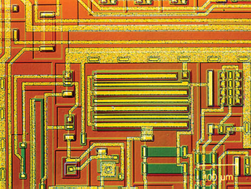
Fig. 1: Detail of a linear IC with conducting leads, resistors, vias and capacitors in the center
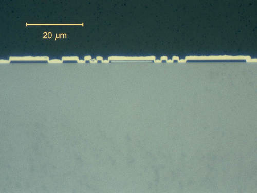
Fig. 2: Cross section of a silicon wafer with conducting leads of an IC
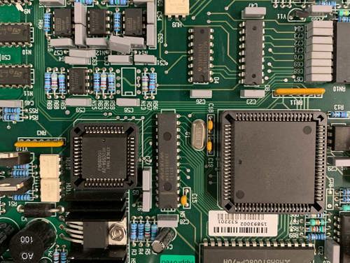
Fig. 3: Components mounted on a PCB
Microelectronic components contain various materials, such as glass, ceramics, metals, and polymers with widely differing properties. Sample preparation therefore requires controlled material removal to reveal the individual characteristics of these materials.
Typical checks include:
- Size and distribution of defects: such as voids, inclusions and cracks
- Bonding and adhesion of materials and their interfaces
- Dimensions and shape of the different parts in the package: layer thickness, wires, solder meniscus
- Porosity and cracks in ceramics
- Flatness and edge retention (very thin layers between materials are inspected at high magnification)
Due to their size and complexity, microelectronic components can be extremely challenging to prepare for metallographic analysis. As a result, special preparation techniques and equipment are required to ensure the right level of precision during controlled material removal.
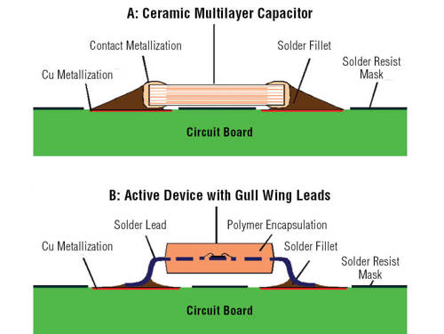
Fig. 4: Example of material compositions in microelectronic components
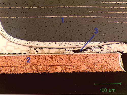
Fig. 5: Multilayer capacitor (1) soldered onto a copper metallization of the circuit board (2); fatigue crack (3) continuously propagating through solder
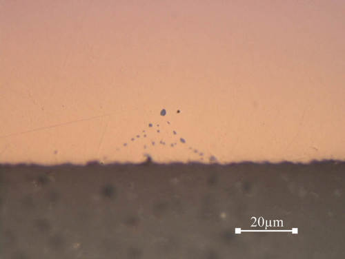
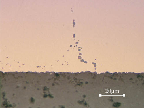
Fig. 6 a & b: Ceramic with copper at high magnification showing difference in flatness: a) initial fine grinding with silicon carbide foil/paper; b) initial fine grinding with diamond on MD-Largo fine grinding disc
Microelectronic sample types
From a materialographic point of view, microelectronics can be divided into three types of samples.
Silicon wafers
The performance of the semiconducting silicon wafer is closely linked to its material properties in terms of microstructure and chemical composition. Therefore, materialographic analysis of silicon wafers is important in both the development of electronic components and quality control.
Through controlled material removal, thin slices of the cylindrical silicon ingot are materialographically prepared for analysis, typically using infrared (IR) microscopy and Fourier-transform infrared (FTIR) spectroscopy. The parallel or cross sections of the silicon wafer are inspected in their non-encapsulated form after accurate materialographic polishing. Details in the integrated circuit are studied in a light or electron microscope, depending on the scale and type of analysis.
Integrated circuits (ICs) and components
The individual wafers are packaged in compact ICs or components, using different interconnections and coating technologies. Materialographic cross sections of these tiny and highly complex microelectronic components are used in development, design, production spot checks and failure analysis. The objective of the examination is to look at cracks, voids, solder balls, conducting and isolating layers, connections, etc.
Metallographic examination often focuses on a particular area inside a package. Controlled material removal, therefore, is employed to identify and reveal this target. Discrete components, such as capacitors, resistors, etc., are also subject to materialographic examination to analyze for geometric and microstructural imperfections.
Printed circuit boards (PCBs)
PCBs consist of a base sheet of epoxy/fiberglass or ceramics, plated metallic layers of copper, and plated holes (also referred to as ‘vias’).
Sample preparation of PCB materials is performed to help locate defects in the substrate material. According to leading industry standards, the quality of a PCB-plated via must be inspected materialographically. For this purpose, a test coupon is produced and prepared so that the center of the plated via can be inspected using a microscope. Additionally, connections, coating coherence and thicknesses are studied, usually in cross sections.
Microelectronic sample preparation challenges
There are three main challenges when performing controlled material removal and target preparation of microelectronic samples.
The miniature dimensions require specialized equipment and accessories suitable for handling small samples. Steps such as cutting and grinding require greater accuracy than normal, due to the dimensions, which are usually in the µm range.
Complex material compositions are common in microelectronics, where soft metals, ceramics and composites are often closely packed. This makes the choice of preparation methods and parameters a compromise, carefully selected to meet the specific requirements.
Controlled material removal and accurate preparation are needed when small targets are the subject of the examination. A metallographic sample inspection often includes looking at a particular area inside a package of interconnected chips. This can be time consuming, as it typically involves a manual controlled material removal process known as ‘grind-and-look’ (i.e. repeatedly grinding and then checking until the target appears and is ready to be polished).
In research or failure analysis, missing the target during a grind-and-look process can mean losing a unique and/or costly sample. Therefore, automated or optimized solutions are increasingly used due to their high mechanical precision, optical measuring units and mechanical stops.
Common difficulties during the preparation of microelectronic samples, include:
- Cutting: Chipping and cracking of silicon wafers, glass or ceramics
- Mounting: Mechanical deformation and thermal damage
- Grinding: Fracture of brittle constituents such as glass fibers or ceramics
- Polishing: Smearing of soft metal layers; relief due to the difference in hardness of different materials; silicon carbide and diamond particles remaining in solder
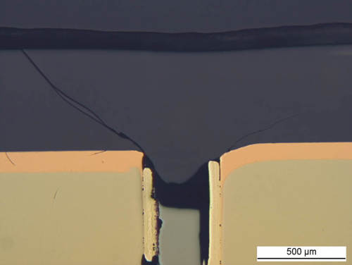
Fig. 7: Detection of a crack in a diode
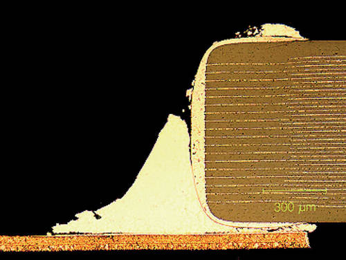
Fig. 8: Through section of an aged ceramic multilayer capacitor with fatigue cracks in the solder connection
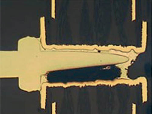
Fig. 9: Large void in the solder of a plated through-hole connection (50 x)
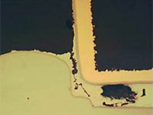
Fig. 10: Void and crack in the solder connection of a plated through-hole (200 x)
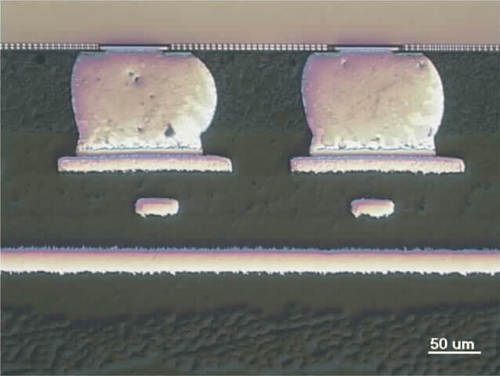
Fig. 11: Cross-section of solder balls, DIC
Preparation of microelectronics: Cutting & mounting
Cutting microelectronic samples
Depending on the size and fragility of the microelectronic component or assembly, mounting prior to cutting may be necessary in order to hold the parts or components together and so avoid mechanical damage.
When cutting, ensure you place the cut far enough from the area of observation to avoid mechanical damage. Once the sample is sectioned, carefully grind away remaining material. This approach will limit the risk of introducing cracks in ceramic, chips in glass, or causing delamination of layers or solder spot.
When cutting microelectronics, you can choose between range of precision cut-off machines, depending on the type of microelectronic sample being investigated:
- For cutting plastics: We recommend an electroplated diamond wheel (E1D20) or a resin-bonded diamond wheel (B0D20)
- If the components are large: We recommend a Secotom with an electroplated diamond wheel (20 mm diameter, or 15 mm for a finer cut)
- For sectioning individual, small or fragile components: We recommend the Accutom, although smaller cut-off wheels can be used
- For a mobile phone or a board mounted with microelectronic components: We recommend a medium-sized machine, such as Secotom
Mounting microelectronic samples
Microelectronic components are not suitable for hot compression mounting, due to their composite and fragile nature. Therefore, they are always cold mounted. However, some acrylic cold mounting resins should be avoided, as they develop high curing temperatures, which can influence solder and polymers, and have high shrinkage, which can crack silicon wafers.
Mounting methods differ depending on the analytic method used:
- For regular mounts for optical microscope: use transparent epoxy resins (ProntoFix, EpoFix)
- To fill voids and holes: use vacuum impregnation
- When using long pass blue and short pass orange filters in an optical microscope: mix a fluorescent dye (EpoDye) with the epoxy, as this gives an excellent contrast to voids and cracks
- For very small vias: use a transparent resin with low viscosity that flows easily into the holes
Find out more
- Get more knowledge, expertise and insight in our cutting and mounting sections.
- See our range of cutting and mounting equipment.
- Get cutting and mounting consumables and accessories.
Preparation of microelectronics: Grinding & polishing
Depending on the size of the microelectronic components and the number of samples required, there are three types of grinding and polishing methods: manual, semi-automatic and fully automatic.
Avoid plane grinding with course abrasives, as this can damage brittle materials and deform soft metals.
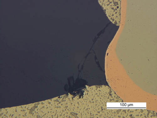
Fig. 12: Crack and fracture damage in glass diode caused by coarse grinding SiC foil/paper
Recommended 3-step process for grinding and polishing of parallel and cross-sections
Step 1
For excellent flatness, fine grind with diamond on a rigid disc (MD-Largo), instead of grinding on silicon carbide foil/paper.
Step 2
To retain flatness after grinding, use diamond polish on a silk cloth. If there are abrasive particles embedded on the soft metal, continue to diamond polish until these are removed.
Step 3
Perform a final polish with colloidal silica (OP-U NonDry), but keep it brief to avoid relief.
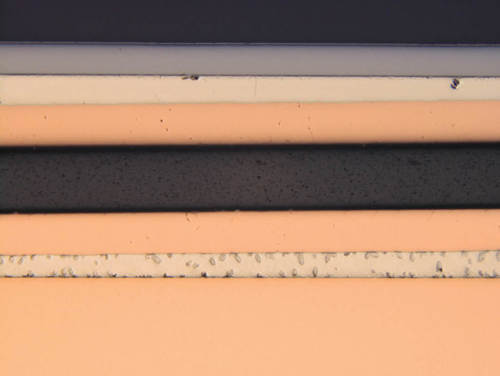
Fig. 13: Relief from polishing due to different hardnesses of materials

Fig. 14: Diamond particles in solder
Manual preparation of microelectronic samples
For manual preparation of non-encapsulated silicon wafers and packages, Tripod is a helpful tool when using the grind-and-look controlled material removal method. For this method, abrasive films with grain sizes from 30 µm to 0.05 µm are mounted on a glass plate, and the specimen is manually ground and polished.
Semi-automatic target preparation of microelectronic samples
For semi-automatic controlled material removal, use silicon carbide foil/paper. We recommend using special sample holders for both mounted and unmounted microelectronic components, such as AccuStop or AccuStop-T. Once several specimens have been ground to approximately 50 µm before the target, remove them from the AccuStop holder and place them individually in the semi-automatic machine for fine grinding and polishing.
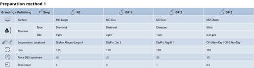
Table 1: Preparation method for microelectronic components, mounted, 30 mm dia.
Fully automatic target preparation of microelectronic samples
We recommend using an automatic machine, such as theTargetSystem for a fully automated controlled material removal process. The total preparation process, including cutting, takes 45-60 minutes.
The TargetSystem aligns and measures the sample prior to preparation and then automatically grinds and polishes it, using video for visible targets and X-ray for hidden targets. It can be used for controlled material removal in both cross and parallel sections of mounted and unmounted samples and has an accuracy of ±5 μm.
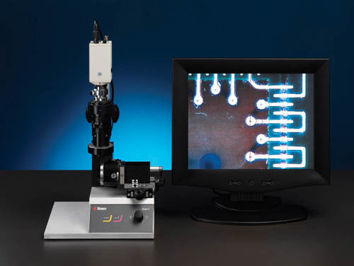
Fig. 15: Target-Z video for positioning and measuring visible targets
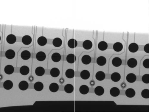
Fig. 16: X-ray of sample with hidden targets
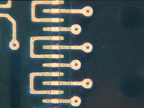
Fig. 17: Sample with visible target, shown using video
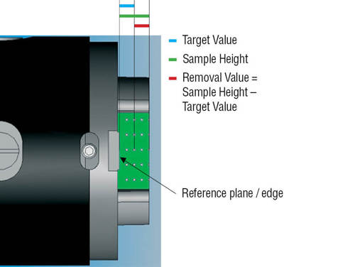
Fig. 18: Holder with sample indicating distances, which are automatically measured and calculated
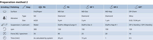
Table 2: Preparation method for target preparation of a microelectronic component
Get proven methods in our e-Metalog
Your choice of grinding and polishing surfaces and suspensions should be dictated by your removal rate, planeness, relief, edge retention and smearing requirements. To help you choose the best method, our e-Metalog contains around 25 proven methods for electronic components, covering a broad selection of materials combinations and preparation requirements.
- Check out the Methods
Find out more
- Get more knowledge, expertise and insight in our grinding and polishing section.
- See our range of grinding and polishing machines and equipment.
- Get consumables and accessories for metallographic grinding and polishing.
Etching of microelectronic samples
Microelectronic components contain different materials and each material reflects light differently. This usually provides enough contrast to render etching unnecessary. However, if etching is required, we recommend a final polish with colloidal silica, as it gives a slight attack on solder and copper. For the final polishing step, use OP-S NonDry suspension with a small amount of hydrogen peroxide (3%). Check your sample after 30 seconds to avoid over-etching. If you need to continue beyond this point, do so gradually.
Our recommendation for etchant for copper and copper alloys in microelectronics:
25 ml water
25 ml ammonium hydroxide
0.5-10 ml hydrogen peroxide (3%)
To further enhance the contrast of the structure, we recommend the following illumination techniques:
- Dark field: for identifying cracks in ceramics
- Differential interference contrast and polarized light: to increase contrast or the color of specific material structures
Download the full application note including preparation methods
Summary
ICs, silicon wafers, and PCBs are key building blocks in modern electronic devices, and metallography plays an important role in the design, development, and failure analysis of these electronic components.
However, ICs, silicon wafers, and PCBs can be challenging to prepare for metallographic analysis. ICs are tiny, with complex geometries, and often include a number of different materials, such as metal, glass, or ceramics. This makes controlled material removal time-consuming, and it requires patience and skill to grind and polish to a specific target inside a component.
There are special tools (AccuStop) that simplify the manual and semi-automatic controlled material removal process. For fully automatic target preparation, the Struers TargetSystem offers fast and precise grinding and polishing. To avoid relief between hard and soft layers and materials, we recommend grinding with diamond on rigid discs and diamond polishing on hard cloths.
Etching is usually unnecessary in microelectronic components. However, if etching is required, we recommend a final polish with colloidal silica, as it gives a slight attack on solder and copper.
Get insight into other materials
Learn more about the materialography of other metals and materials. Check out our materials page

All images by Kelsey Torboli, Applications Engineer, USA
For specific information about the metallographic preparation of microelectronics, contact our application specialists.